NIL Characterisation as a Service
Precise and reproducible nanoimprint lithography depends on the accurate characterization of surfaces, layer thicknesses, and micro- and nanostructures.
With many years of experience and state-of-the-art metrology infrastructure, we provide comprehensive analysis across a broad range of parameters to support your project.
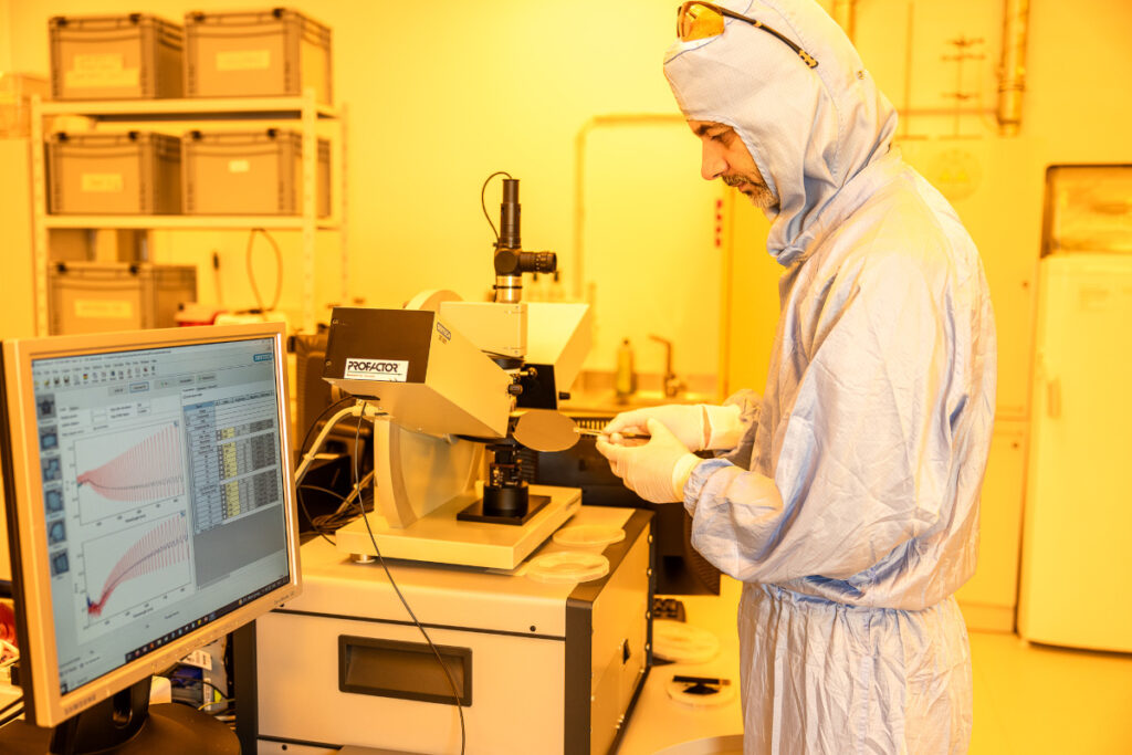
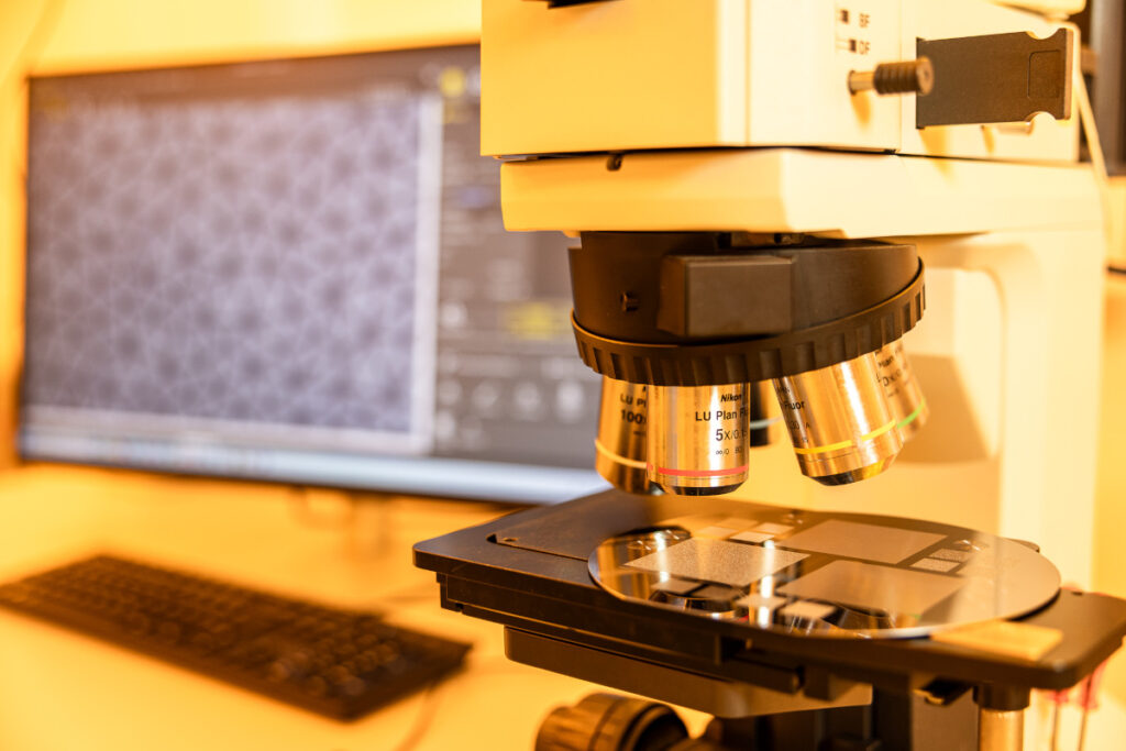
Advanced metrology equipment
- Atomic Force Microscope (AFM) – Bruker Dimension Edge: High-resolution surface topography at the nanoscale.
- Optical Microscope – Keyence VHX-5000: Flexible optical inspection with deep focus imaging.
- Profilometer – Veeco Dektak 150: Accurate step height and film thickness measurements.
- Plasma Cleaner – Diener NANO: Surface cleaning and activation for improved material adhesion.
- Ellipsometer – Sentech: Measurement of thin film thickness and refractive index.
- 3D Laser Scanning Microscope – Keyence VK-X3000: High-resolution, true-color 3D imaging of microstructures.
- Contact Angle Measurement System – Krüss DSA100: Surface energy and wettability analysis.
- UV/Vis Spectrometer: Spectral analysis of transmission and absorption of thin films.
- Angle-dependent Reflection and Transmission Setup (our own development): Characterization of optical behavior at variable incident angles.
Our metrology services are tailored to the specific needs of nanoimprint lithography — from substrate preparation to process monitoring and final quality control.


