Micro- and Nano-Fabrication
Efficient and scalable with Nanoimprint Lithography (NIL).
Micro- and nanostructures on surfaces enable specific functional and optical product properties – particularly in micro-optics, life sciences, and premium consumer applications.
Conventional structuring methods are often too complex, uneconomical for small batches, and limited in their scalability.
Nanoimprint Lithography (NIL) enables the precise replication of micro- and nanostructures on a variety of substrates. PROFACTOR has helped shape NIL since its early days with a focus on application-oriented process development.
This allows new functional surface properties to be realized and innovative products to be scaled efficiently from prototypes and pilot runs to mass production.
Technologies
Nanoimprint Lithography (NIL)
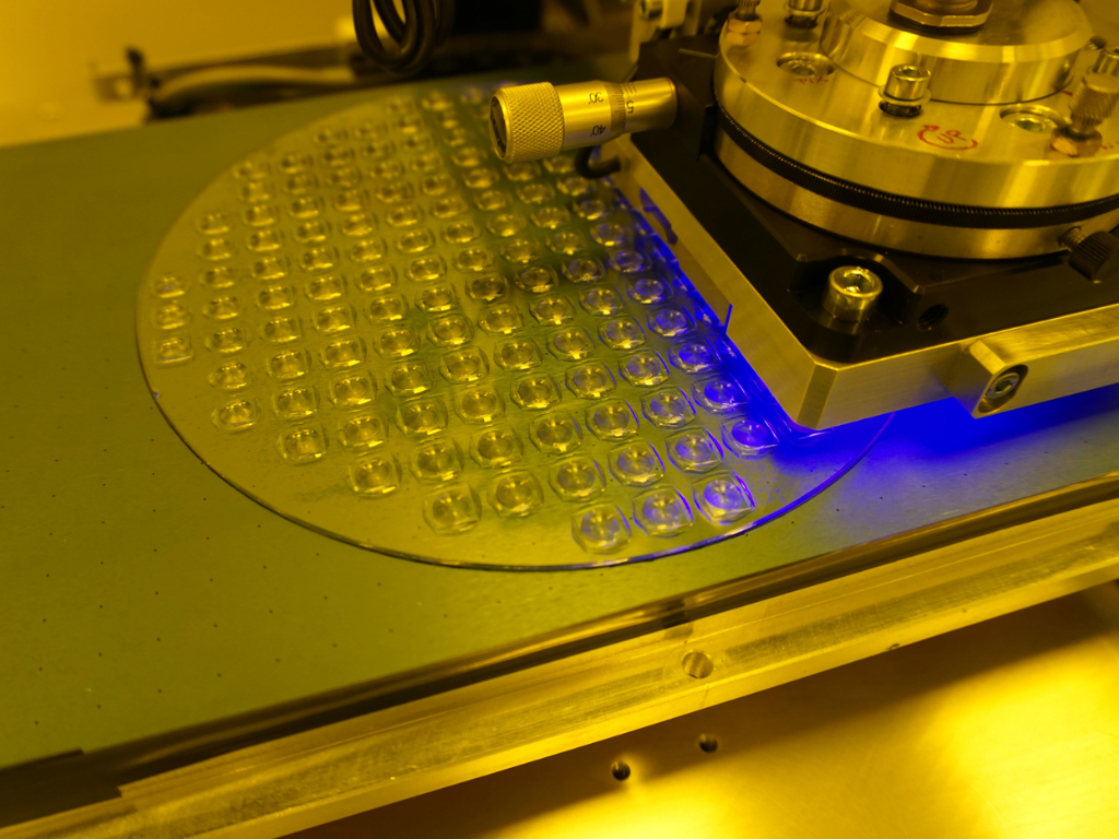
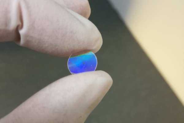
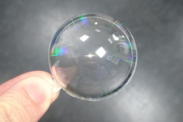
NIL is a mature technique that uses a stamp to transfer micro- or nanopatterns cost-effectively onto substrates such as wafers, glass, ceramics, plastics, or metals.
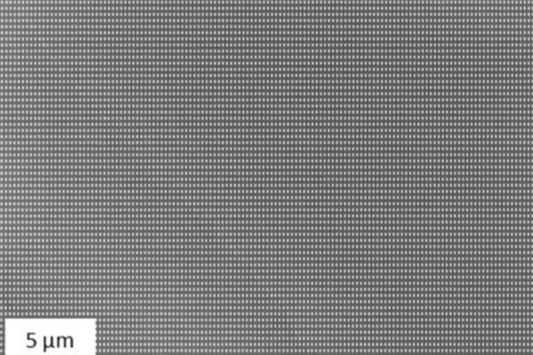
A stamp is pressed with high positional accuracy into an imprint resist and cured via UV light, resulting in a high-precision reproduction of the stamp’s 3D structure.
Depending on requirements for material, throughput, or resolution, PROFACTOR utilizes the following processes:
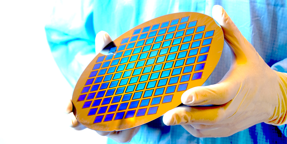
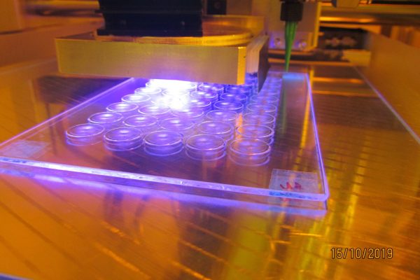
Wafer Level Nanoimprinting
Large-scale replication of micro- and nanostructures directly on wafers. This process offers excellent reproducibility with high throughput and high resolution.
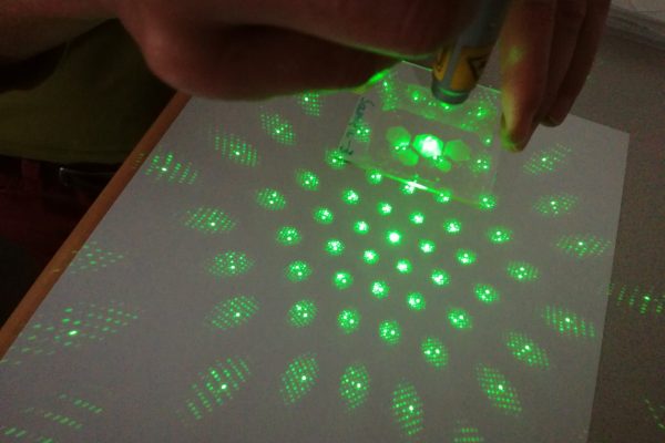
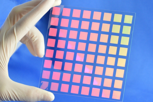
Typical applications include diffractive optics, metasurfaces, microfluidics, sensors, and advanced semiconductor packaging.
Roll-to-Plate Nanoimprinting
Nanostructures are transferred with high accuracy from a roll to a polymer film on a substrate.
Due to its high throughput and replication quality, this method is particularly suitable for the mass production of optical components like diffraction gratings and metasurfaces.
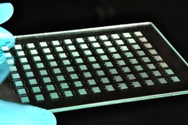
Step & Repeat Nanoimprinting
Enables the position-accurate replication of high-precision nanostructures from a single stamp onto large-area substrates.
Step & Repeat Nanoimprinting is used both for manufacturing large-area stamps and for producing small quantities of optical, photonic, and microfluidic components.
Solutions for Precise Micro- and Nanostructures
Our proven nanoimprint technology platform forms the basis for the efficient development and production of your micro- and nanostructures.


Added Value Through Nanoimprint Lithography
Years of experience enable the efficient development of reliable processes for your micro- and nanostructures.

Replication of complex micro- and nanostructures
High throughput and time savings
Precise production of nanostructures on various materials
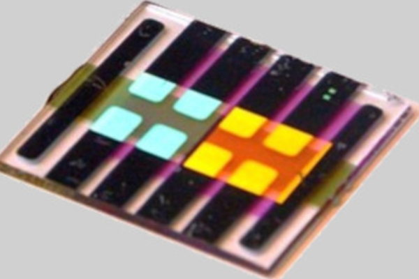
Application Areas
Selected practical examples show the diverse use of the nanoimprint technology:
PROFACTOR, Your Technology Partner
From innovative ideas to industrial implementation.
Requirements, Concept, and Feasibility
After the initial exchange of information, we clarify objectives and initial requirements.
If needed, we test the basic feasibility of the technological solution in the laboratory based on your structure designs.
This creates a shared understanding of the solution concept, along with a rough cost estimate as a basis for the following development stages.
Process Development & Demonstrators
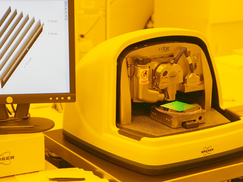
Based on your requirements and technological feasibility, we develop a customized process. We carry out detailed characterizations to safeguard the processes.
Often, process development is divided into several stages with design optimizations and regular coordination.
Finally, we manufacture and deliver the agreed quantity of prototypes, allowing you to test the functionality and quality of the components for the first time.
Small Series & Process Transfer
The process is further developed towards semi-automated production for larger quantities. Proven step-and-repeat or roll-to-plate technologies are used here.
We typically manufacture 100 to several thousand replications of your designs, allowing you to further qualify your product design and carry out initial field tests.
In a further step, we help to transfer the process into your production.
Proven Partnerships
Selected customers and partners from joint development and industrial projects.
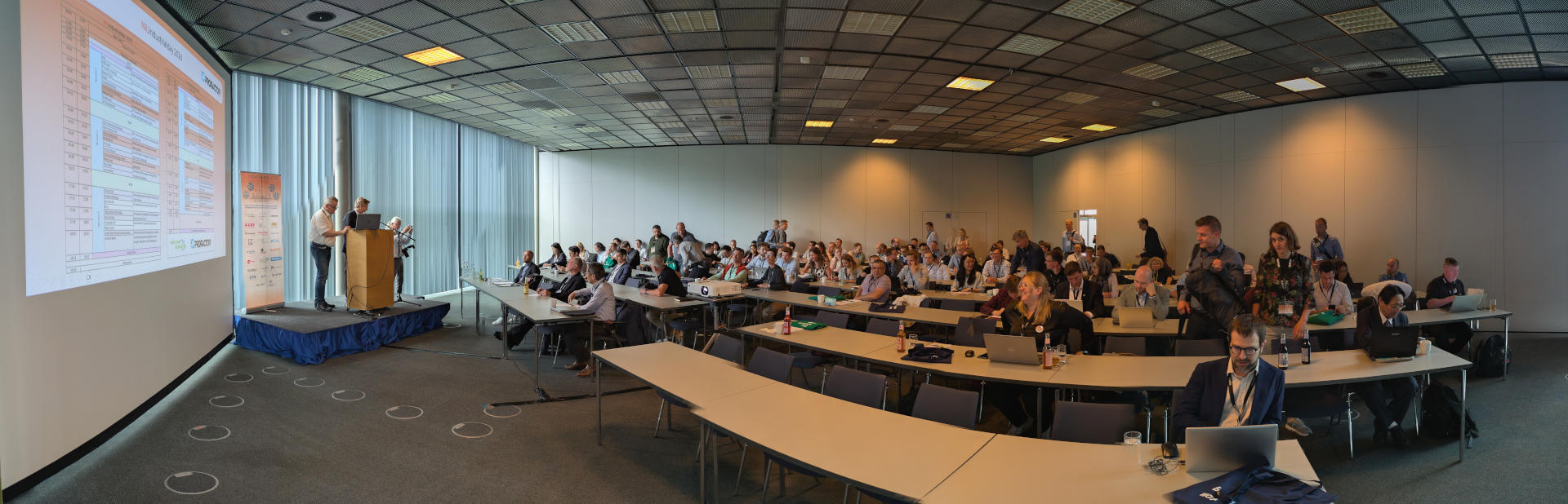
Current Research Projects
Our technology portfolio is based on a large number of research projects with national and international partners from industry, universities and research institutions.
We combine industry requirements and global trends to develop forward-looking research projects. In this way, we work with our partners to ensure the competitiveness of industrial production.

BEES-4-CO2RR
BioStruct
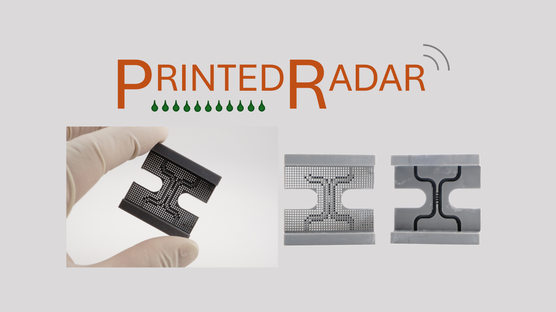
PrintedRadar
Downloads
Nanoimprint Lithography – Advanced Solutions for the Replication of Micro- and Nanostructures

Contact person
Head of Business Development+43 7252 885-252
christoph.brandstaetter@profactor.at